Junction Field Effect Transistor (JFET) is a semiconductor device that comes under the category of field-effect transistor. These types of transistors are operated by an electric field across the junction of the device.
Table of Contents
Types of JFET
In electronics engineering, there are two types of JFET.
- N Channel JFET
- P Channel JFET
1. N Channel JFET
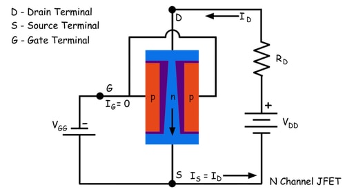
An N channel JFET is made of Si or GaAs bar. The bar is doped with N-type impurities. One metallic terminal is attached to each of both ends of the bar. One of the terminals is called the drain terminal, and the second is called the source terminal. Both sides of the bar are highly doped with P-type impurities. The region which doped with P-type impurities is called the gate region. A metallic terminal is connected to the gate region, and this terminal is known as the gate terminal.

2. P Channel JFET
P channel JFET is made of Si or GaAs bar doped with P-type impurities. The sides of the bar are highly doped with N-type impurities. Here also the drain, and the source terminal are connected to both ends of the bar. The terminal connected to the side N-type region is the gate terminal.
NB:- Here in both types of junction field-effect transistor both drain and source terminal can be interchangeable.
If a voltage is applied between the drain and source terminal, a current starts flowing through the device. The space between two oppositely doped regions is referred to as the channel of the device. The current flows through the channel due to the drift of the majority of carriers. The majority of carriers enter into the channel through the terminal is referred as to the source terminal and the terminal through which the majority of carriers leave the channel is referred to as the drain terminal.
In normal operating conditions the drain terminal of N channel JFET is applied with positive potential and the drain terminal of a P channel JFET is applied with negative potential. The gate voltage is kept such in a JFET that the PN junction between the gate region and the channel is in reverse biased condition. The width of the depletion layer of this PN junction can be varied by varying gate terminal voltage. The opening of the channel depends on the width of the depletion layer. If by Changing the gate terminal voltage, the width of the depletion layer is enhanced, it is expanded into the channel and decrease the opening of the channel, and therefore the current through the channel gets reduced. Thus, we can conclude that by controlling gate voltage we can control the drain current. Depending on that common property of the JFET we can utilize this JFET for various electronic applications. A JFET can be used as a switch, as an amplifier, etc.